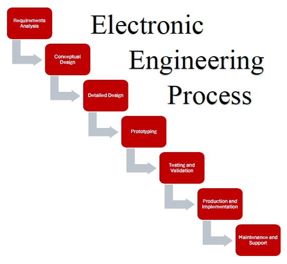
Electronics engineering process steps
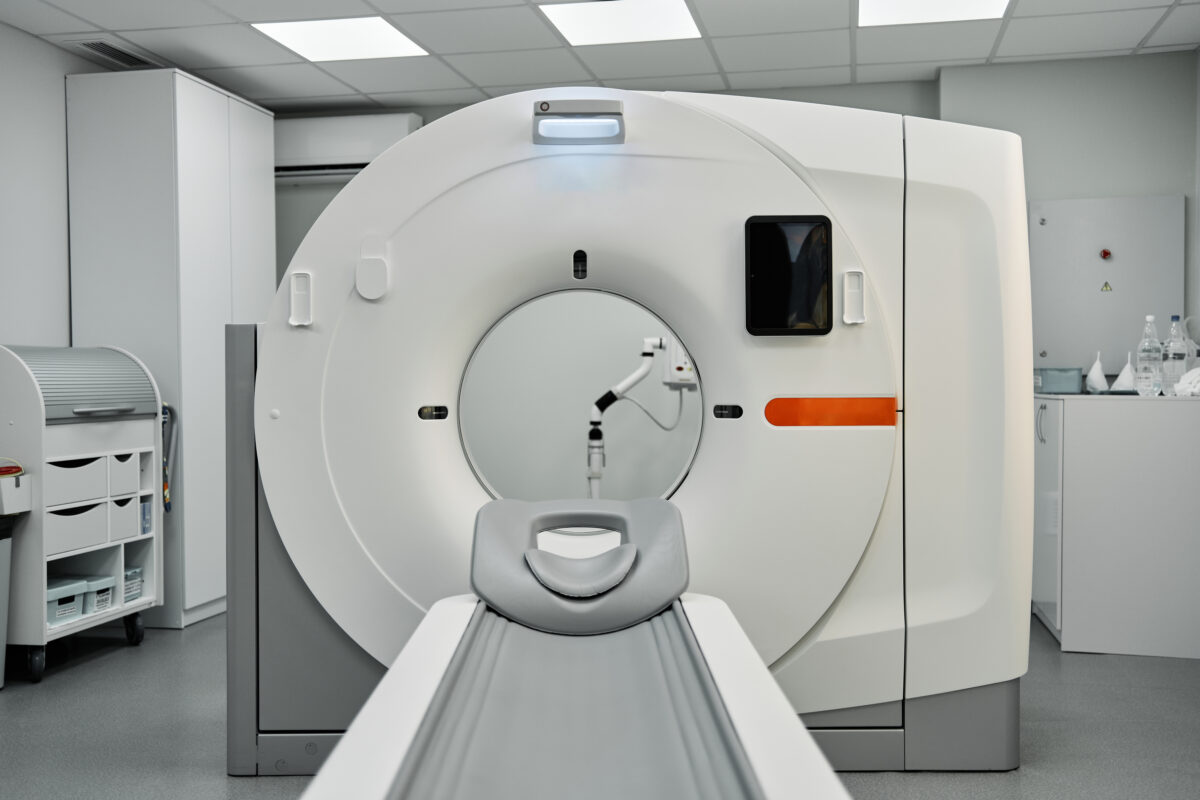
Technology is evolving at an unprecedented pace. As a result, the demand for efficient and innovative electronic devices and systems is more crucial than ever. The electronic engineering process plays a pivotal role in ensuring that engineers can optimize design to help facilitate efficient manufacturing and ensure electronics operate reliably.
Major Steps of the Electronic Engineering Process
Understanding the electronic engineering process is crucial in helping engineers optimize electronic device design. The table below delves into the key steps in the process.
Engineering Process Optimization
Optimizing electronic device design involves a combination of strategies and techniques that engineers can use to improve performance, efficiency, and usability while minimizing costs and time to market. Here are several key approaches:
Simulation and Modeling
- CAD Software: Engineers can use computer-aided design (CAD) tools to create models of electronic components, which enables simulation of their behavior under various conditions.
- Circuit Simulation: Tools like SPICE enable engineers to simulate circuit performance and analyze signal integrity, thermal performance, and power consumption.
Component Selection
- Component Choice: Selecting high-quality components that meet device specifications can greatly enhance performance. Engineers should consider factors like power ratings, tolerance, and thermal characteristics.
- Integration: Using integrated circuits (ICs) can simplify designs and reduce the number of components, leading to smaller sizes, lower costs, and improved reliability.
Thermal Management
- Heat Dissipation: Proper thermal management using heat sinks and thermal pads is vital in preventing overheating and ensuring device longevity.
- Thermal Simulation: Tools to simulate thermal performance help engineers understand heat distribution and identify potential hotspots.
Power Optimization
- Energy Efficiency: Engineers design circuits and select components that minimize power consumption, such as using low-power microcontrollers or optimizing switching regulators.
- Power Management ICs: Implementing specialized ICs that manage power distribution and consumption can significantly enhance battery life in portable devices.
PCB Layout Optimization
- Design for Manufacturability (DFM): Optimizing the printed circuit board (PCB) layout for manufacturing processes can reduce production costs and improve yields.
- Signal Integrity: Proper routing of signals, minimizing trace lengths, and managing impedance helps prevent issues such as crosstalk and reflections.
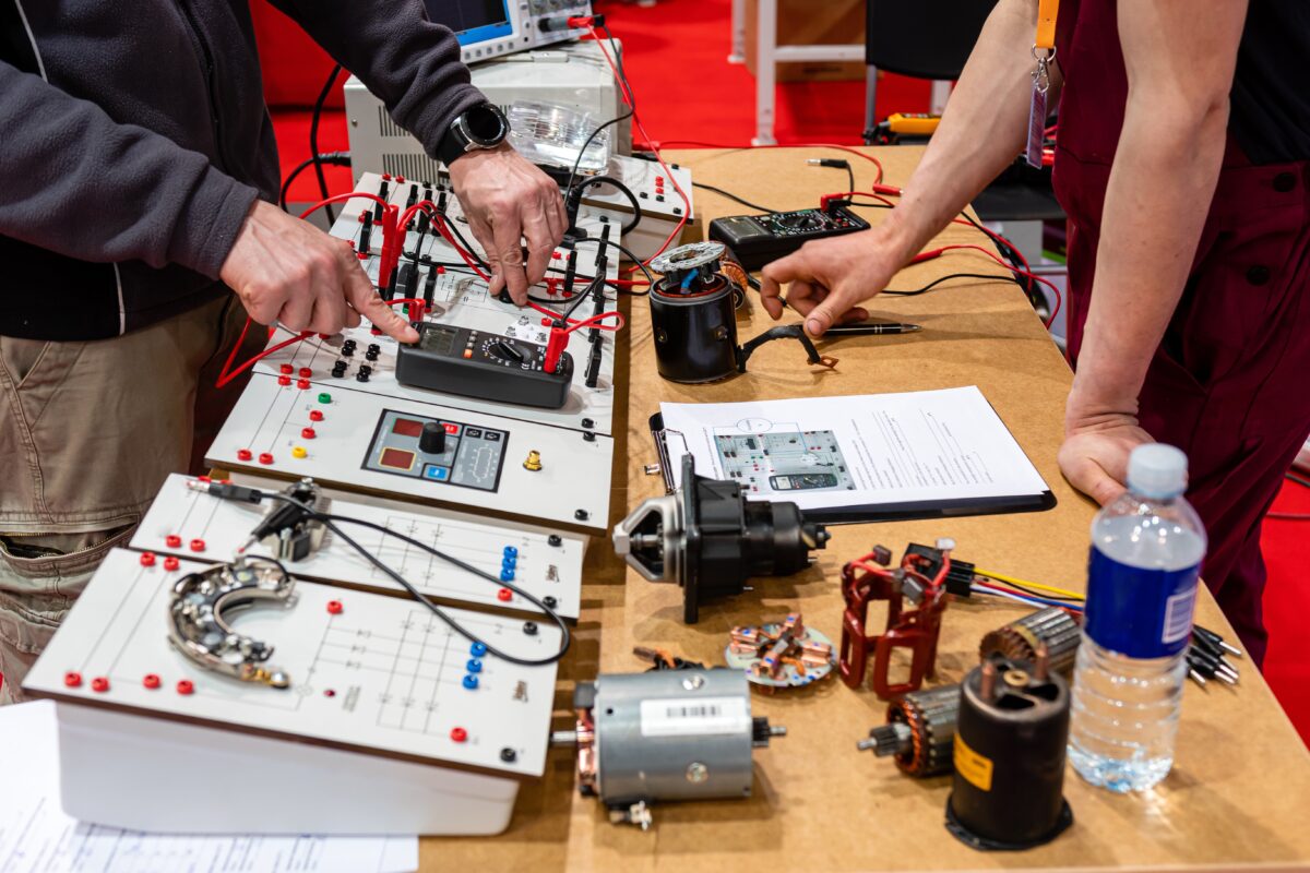
Testing and Iteration
- Prototyping: Rapid prototyping allows engineers to test and iterate on designs quickly. Feedback from prototypes helps refine designs to meet performance and user needs.
- Validation: Thorough environmental and stress testing ensures that the device will perform reliably in real-world conditions.
User-Centric Design
- Ergonomics: Understanding user interactions helps engineers design device interfaces and controls that enhance usability and accessibility.
- Aesthetics and Form Factor: Designing a product that is functional and visually appealing can increase marketability.
Cost Considerations
- Material Selection: Using cost-effective materials without compromising quality can significantly reduce production costs.
- Scalability: Designing for scalability ensures that production can be ramped up or down efficiently based on demand.
Sustainability
- Eco-friendly Materials: Selecting sustainable components, materials, and processes can reduce environmental impact.
- End-of-life Considerations: Designing for disassembly and recycling can enhance the sustainability of electronic products.
Understanding the electronic engineering process and the techniques employed to optimize it is a window into the engineering mindset that can be leveraged to improve engagement with experienced designers and the next generation of innovators that will drive PCB design. This includes meeting engineers where they are and delivering pertinent content that helps them work more effectively and efficiently. To reach the greatest number of engineers, you should rely on the most trusted online resource for sourcing component CAD models and design information, Ultra Librarian.
Unlock faster innovation and optimal outcomes with Accelerated Designs. With access to the latest EDA software, diverse data, and the industry’s most comprehensive PCB CAD-content digital library, we provide the tools, technologies, and expertise to reduce development costs, speed time to market, and overcome common design challenges. Contact Accelerated Designs to start optimizing your design process today.